Manufacturer of Optical Spectrometers, Camera Systems for OEM Industrial Applications
Hyperspectral Imaging Spectrometer Applications
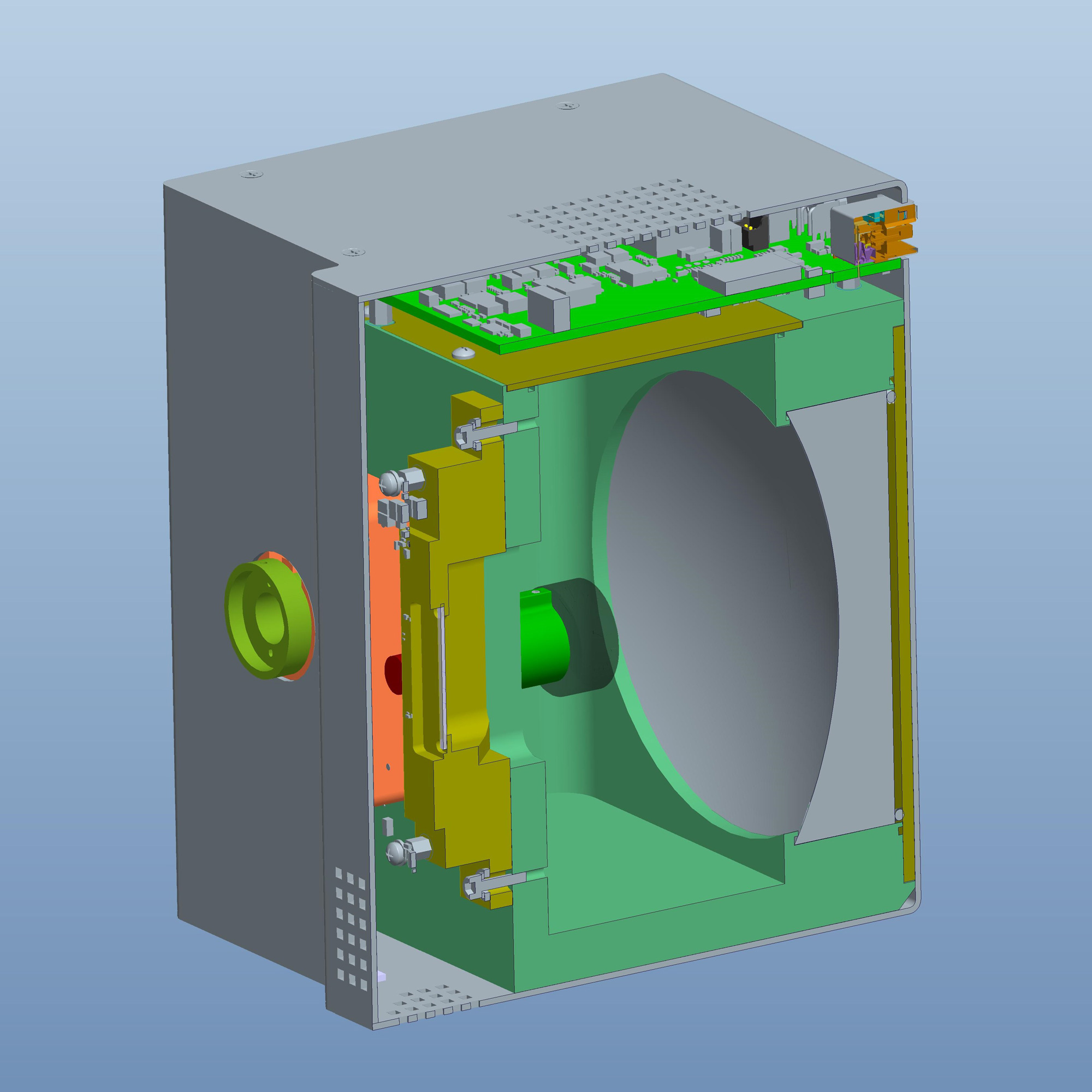
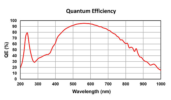
HORIBA has developed a unique hyperspectral imaging spectrometer with an integrated scientific CMOS camera (12-16 bit) featuring HDR (95dB Dynamic Range and 1.7e- noise) and 95% Q.E peak efficiency:
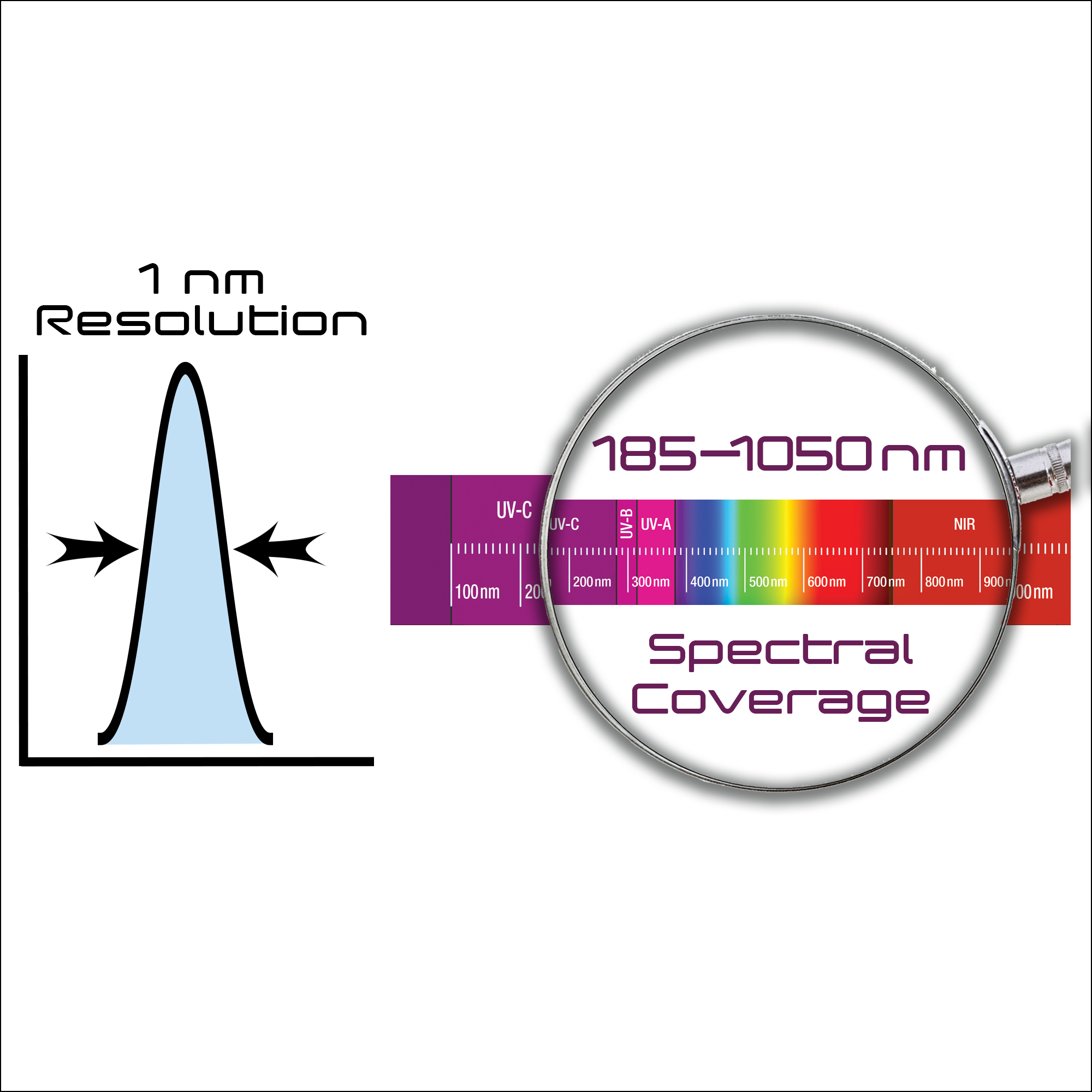
PoliSpectra® H116 features broad UV-NIR coverage in one acquisition (185-1050 nm) combined with the highest spectral resolution (<1 nm).
The elegant all-concentric design combines high spatial and spectral resolution using a type-I holographic diffraction grating. This system is used as a line-scanning instrument (push-broom) that collects full spectral data simultaneously, across the input slit height at 188 frames per second (or higher with AOI/binning).
For OEM hyperspectral and multispectral applications
ㆍ Remote Sensing (Aerial - drone/uas/uav or aircraft…)
ㆍ Quality Control Inspection / Optical metrology in Semiconductors
ㆍ DNA sequencing / Capillary Electrophoresis / PCR
ㆍ Process Monitoring by Reflectometry, Emission, Raman, Fluorescence…
ㆍ Microscopy (Mapping, Complete custom solutions)
ㆍ Advanced Machine Vision / Industrial camera
ㆍ Recycling (Sorting and quality control in recycling plants)
ㆍ Food & Beverage Inspection
ㆍ Superb imaging quality
ㆍ Frame rates as fast as 188 fr/s
ㆍ High spectral and spatial resolution at F/2.3
ㆍ High throughput combined with low stray light performance
ㆍ 2D Scientific CMOS with high quantum efficiency and low noise
ㆍ Broad wavelength coverage from 185 nm to 1050 nm
ㆍ Stable and robust
Thermal stability study cycling from -20ºC to 50ºC
![]()
Scientific CMOS Back-Illuminated Sensor Quantum Efficiency
Hyperspectral Imaging Distortions: Keystone and Smile

OEM Spectrometer Selection Guide

General Spectrometer Specifications*
| Spectral Coverage | 185–1050 nm Tunable at factory between these ranges: 185-920 nm and 280-1050 nm |
| Spectral Resolution | 1.25 nm typical (22 μm slit width) and up, depending on the slit size |
| Spatial Resolution | 50 µm typical |
| Spectral Dispersion | 34.6 nm/mm; 0.38 nm/pixel |
| Focal Length | 116 mm |
| F/# | F/2.3 |
| Smile and Keystone | 1.5 pixel (typical) |
| Stray Light** | < 0.1% (typical) |
| Wavelength Accuracy | 0.1 nm (using multi-area wavelength calibration) |
| Software | LabVIEW™ acquisition software for initial evaluation (DLLs provided for software integration) |
Specifications for Scientific Back-Illuminated CMOS Image Sensor with High Speed Electronics
| Detector Model | sCMOS BI sensor with electronic rolling shutter (All the parameters are specified at normal room temperature of 25º C unless otherwise noted) | |
| Sensor Format*** | 2048 x 512 | |
| CMOS Pixel Size | 11 µm x 11 µm | |
| CMOS Height | 5.6 mm | |
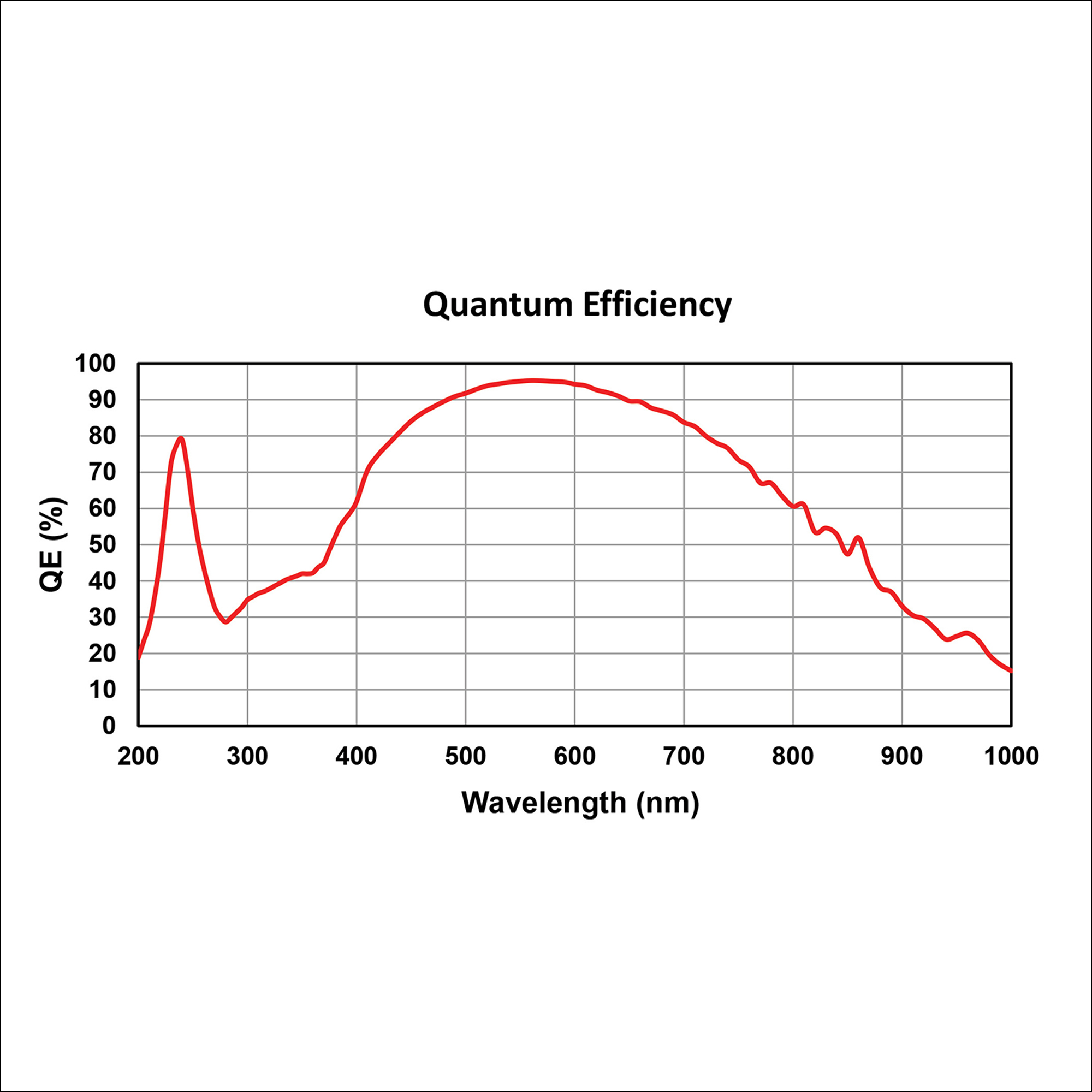
| CMOS QE | The peak QE is 77% at 250 nm and 95% at 560 nm (refer to graphs below) | |
| Thermoelectric Cooling | Uncooled | |
| Frame Rate | 94 fps (HDR mode), 188 fps (STD mode) on 2D sCMOS sensor | |
| Full Well | 80 ke¯ typical (HDR mode) | |
| Readout Noise | 1.6 e¯ typical, 2.0 e¯ maximum | |
| Digitization | 16-bit (HDR mode), 12-bit (High Sensitivity mode | |
| Dynamic Range (HDR mode) | 93.9 dB typical in HDR mode | |
| Non-linearity (measured on each system) |
< 1.8% (maximum) in HDR mode | <0.9% (maximum) at high gain |
| Communication | USB 3 | |
| Environmental Conditions | Operating temperature 15° C to 40°C ambient; Relative humidity <70% (non-condensing); Storage temperature -25° C to 45° C |
|
| Power requirements AC/DC Power Supply (provided) |
90-264 VAC, 47–63 Hz | |
* Specifications, form factor, and spectrometer cover subject to change without notice. No LabVIEW license is needed to run our acquisition software.
** Stray light using BP Filter: Baseline light level, outside the band, divided by BP peak (unsaturated) value.
Scientific CMOS Back-Illuminated Sensor Quantum Efficiency

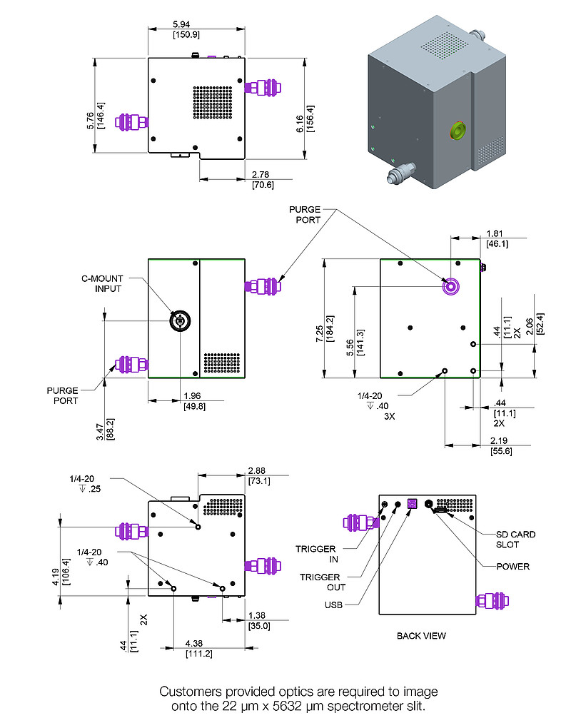
Mechanical Drawings
