Compact High Resolution CMOS or CCD Spectrometer
MiniVS70 is the latest evolution of the cost-effective high performance family of mini-spectrometers from HORIBA Scientific. This MiniVS70 system for industrial applications uses a modified miniaturized VS70 optical engine which is optimized for the UV-VIS-NIR spectral range. The MiniVS70 is based on a high performance aberration corrected concave grating fitted with a custom order-sorting filter to eliminate higher orders.
This platform is specially designed to easily adapt to a large variety of detectors and electronic drivers. The optical design is optimized to minimize stray light and maximize optical performance. The MiniVS70 outperforms competitive mini-spectrometers based on front-illuminated CMOS linear sensors or low-cost back-illuminated CCDs.
For OEM Industrial Applications
ㆍ Fluorescence, Emission and Reflectance
ㆍ Examples :
- Semiconductors
- Analytical Chemistry
- Process Monitoring
- Medical Analysis (blood, DNA, etc.)
- Metrology
- Chemical Fingerprint by Plasma Analysis
ㆍ High spectral resolution
ㆍ Compact size, robustness, and stability
ㆍ Configurable with linear CMOS for affordability, or CCD for highest sensitivity
ㆍ Various wavelength ranges UV-VIS / VIS / UV-NIR
ㆍ Ultra low stray light
ㆍ Highly customizable for many applications
ㆍ High volume production capacity
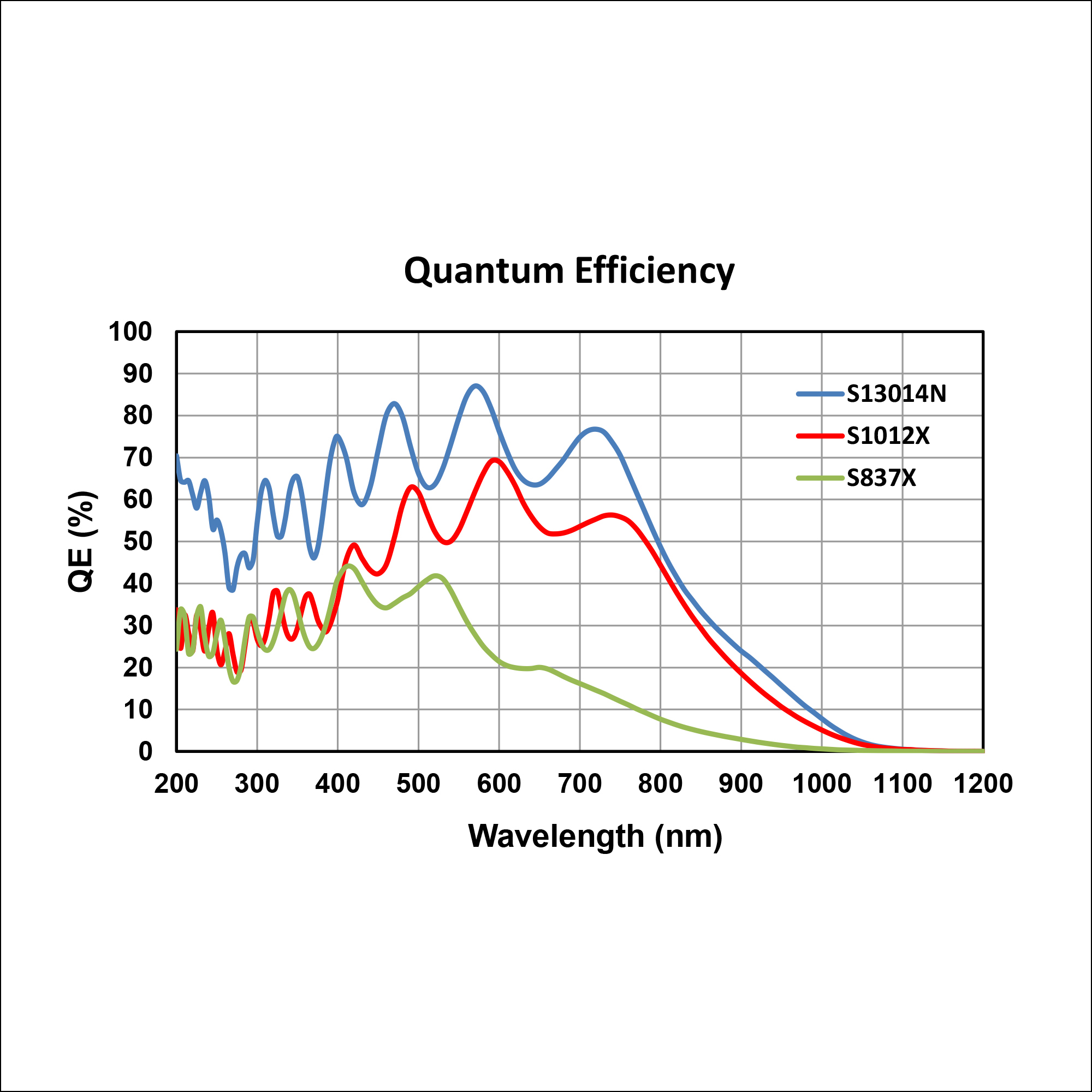
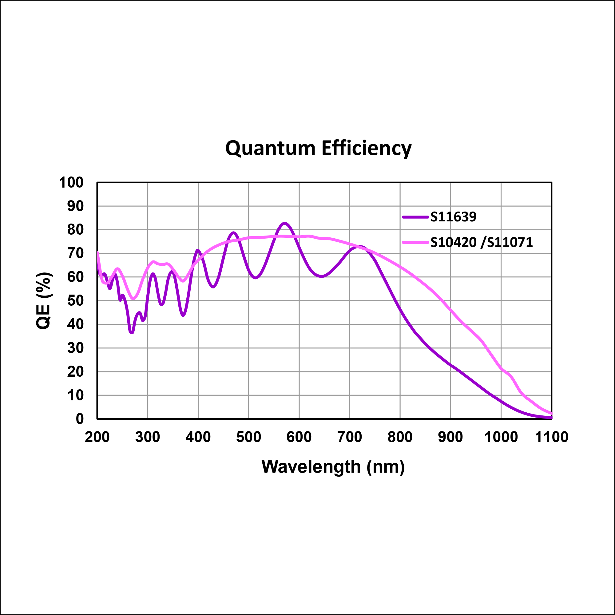
Quantum Efficiencies
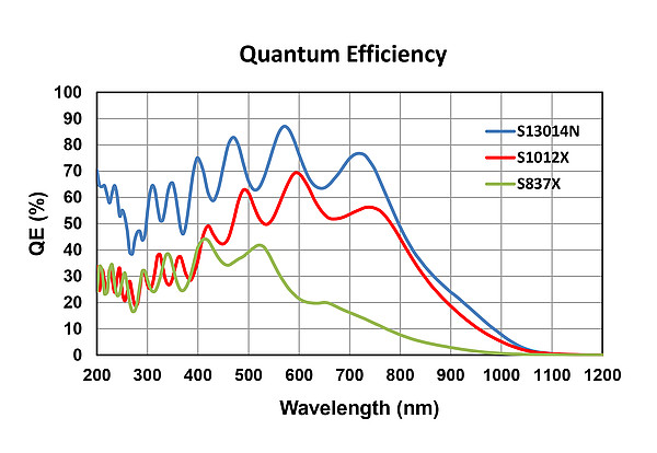
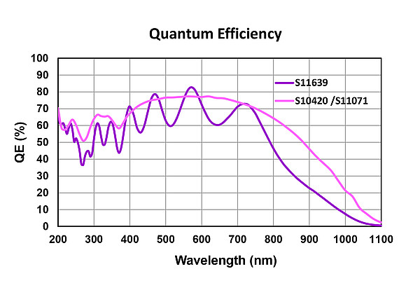
CCD Selection Guide

| General Spectrometer Specifications* | |
|---|---|
|
Spectral Coverage |
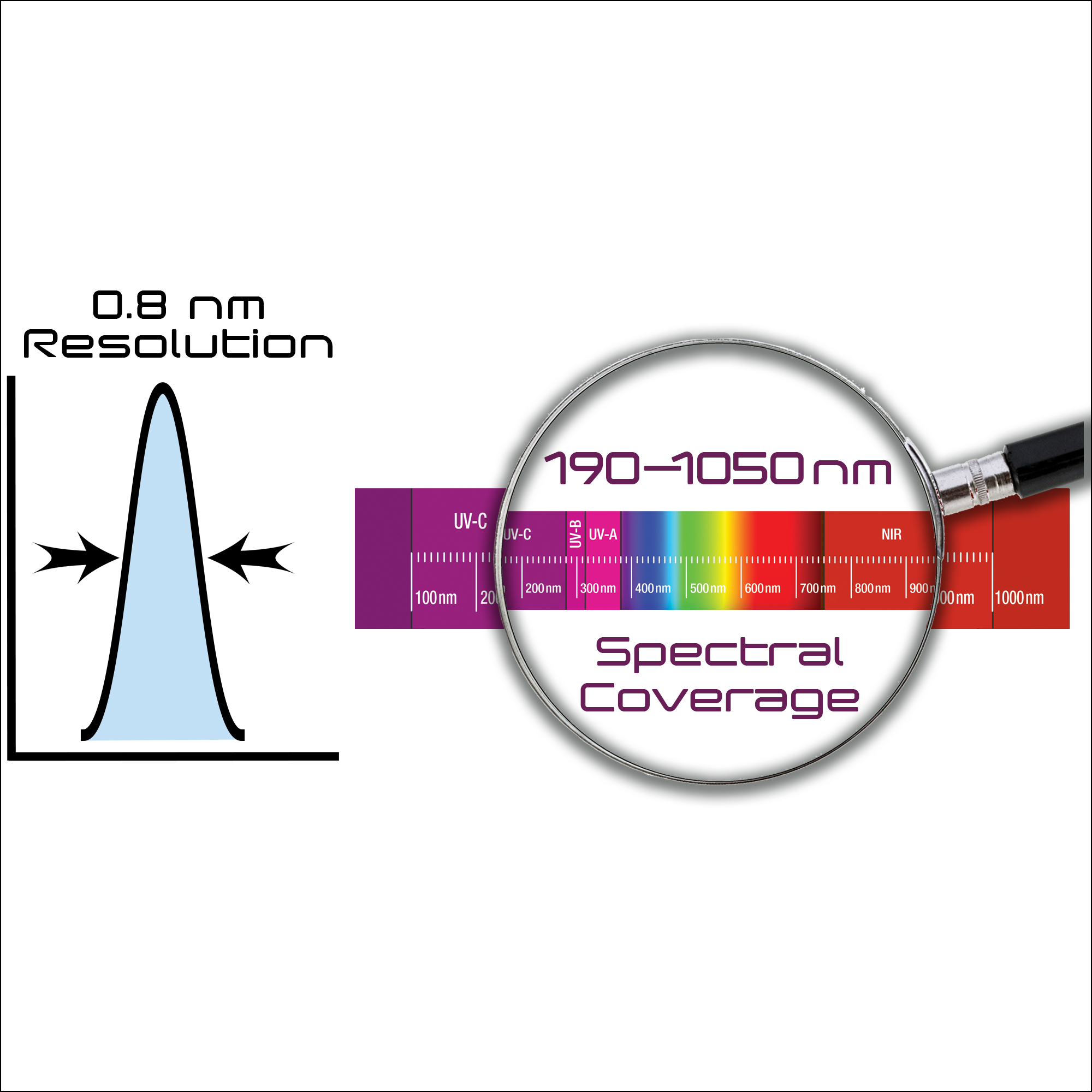
200 - 1050 nm with double-blazed 365 l/mm grating, 190 – 850 nm with 477 l/mm grating, ≤ 400 – ≥ 800 nm with 582 l/mm grating |
|
Spectral Resolution |
2 nm for 365 l/mm grating, 1 nm for 477 l/mm grating, 0.8 nm for 582 l/mm grating (25 μm slit for all) |
|
Average Spectral Dispersion |
30.9 nm/mm for 365 l/mm grating, 23.7 nm/mm for 477 l/mm grating, |
|
Focal Length |
70 mm |
| Options | Selection of high grade sensors: CMOS, B.I. CCD, PDA Input port: SMA, FC, free space, custom input |
|
F/# |
~ F/3.8 |
|
Wavelength Accuracy |
<0.25 nm (using multi-area wavelength calibration) |
| Stray Light | < 0.1% |
|
Software |
LabVIEW™ acquisition software for initial evaluation (DLLs provided for software integration) |
| Detector Options and Specifications | |||
|---|---|---|---|
| Linear front illuminated CMOS sensor with high speed and UV extension |
Linear back-illuminated CCD with large active area with high sensitivity |
||
| Sensor Type | Hamamatsu CMOS linear image sensor S11639 with active pixel structure and global e-shutter |
Hamamatsu CCD sensor S11071 with high spectral acquisition speed |
Hamamatsu CCD sensor S10420 with high dynamic range |
| Sensor Format | 2048 x 1 pixels | 2048 x 70 pixels, shorter version available on request |
2048 x 70 pixels, shorter version available on request |
| Active Area | 28.7 x 0.2 mm | 28.7 x 1 mm | 28.7 x 1 mm |
| Pixel Size | 14 x 200 μm | 14 x 14 μm | 14 x 14 μm |
| QE | > 60% for 450 - 750 nm | ||
| Full Well Capacity | 100,000 e¯ (typical) 80,000 e¯ (minimum) |
>240,000 e¯ (typical) >175,000 e¯ (minimum) |
>375,000 e¯ (high FW mode) |
| Readout Noise | 16 e¯ (typical) 20 e¯ (maximum) |
35 e¯ (typical) 45 e¯ (maximum) |
50 e¯ (typical) & 75 e¯ maximum) in high full well mode |
| Maximum Spectral Rate | 1400 spectra/s and higher | 770 spectra/s | 223 spectra/s |
| ADC | 16-bit | 16-bit | 16-bit |
| Dynamic Range (FW/RN) | 6250:1 (typical) | 6800:1 (typical) | 7500:1 (high FW mode) (typical) |
| Non-linearity | <0.1% (corrected) | <0.4% (corrected) | <0.4% (corrected) |
| Dark Current (@25° C) | 375 e¯/pixel/s (typical) 500 e¯/pixel/s (maximum) |
50 e¯/pixel/s (typical) 500 e¯/pixel/s (maximum) |
50 e¯/pixel/s (typical) 500 e¯/pixel/s (maximum) |
| Communication | USB 2 | ||
| Environmental Conditions |
Operating temperature +15° C to 45° C ambient Relative humidity <70% (non-condensing); Storage temperature -20° C to 60° C |
||
| Power Requirements | Through USB 2 | Y Cable (5 VDC) | |
Other detector options, such as CMOS-PDAs with passive pixel structure and full well up to 1Ge- available.
| Linear CMOS-PDA Options (other sensors available upon request) | ||
|---|---|---|
| Sensor type | S1012X Series (High Performance) | S837X Series (Low Cost) |
| Pixel Format | 25 or 50 μm pixel pitch; 0.5 or 2.5 mm pixel height; 512 pixels or 1024 pixels | |
| Detector QE | Refer to graphs below | |
| Full Well (e-) | From 94 Me¯ to 1 Ge¯ (typical) | From 43 Me¯ to 430 Me¯ (typical) |
| Readout Noise (e-) | 5200 e¯ (typical) | 3370 e¯ (typical) |
| Spectrometer housing will be slightly different depending on CMOS-PDA options | ||
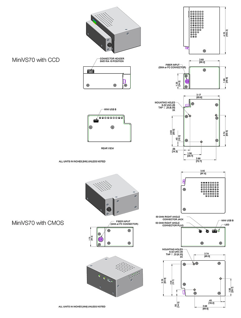
Mechanical Drawings
