Miniature High Throughput Spectrometer
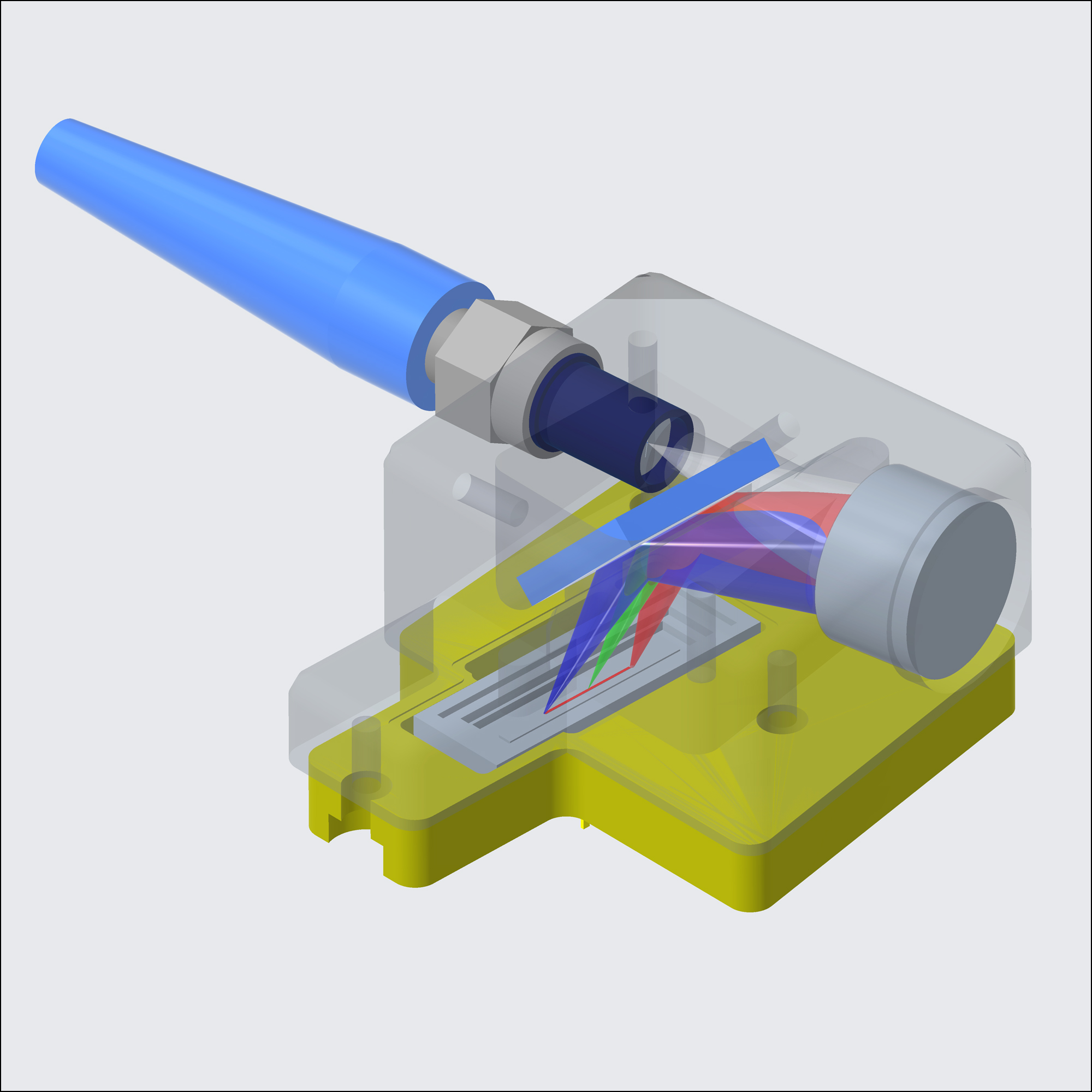
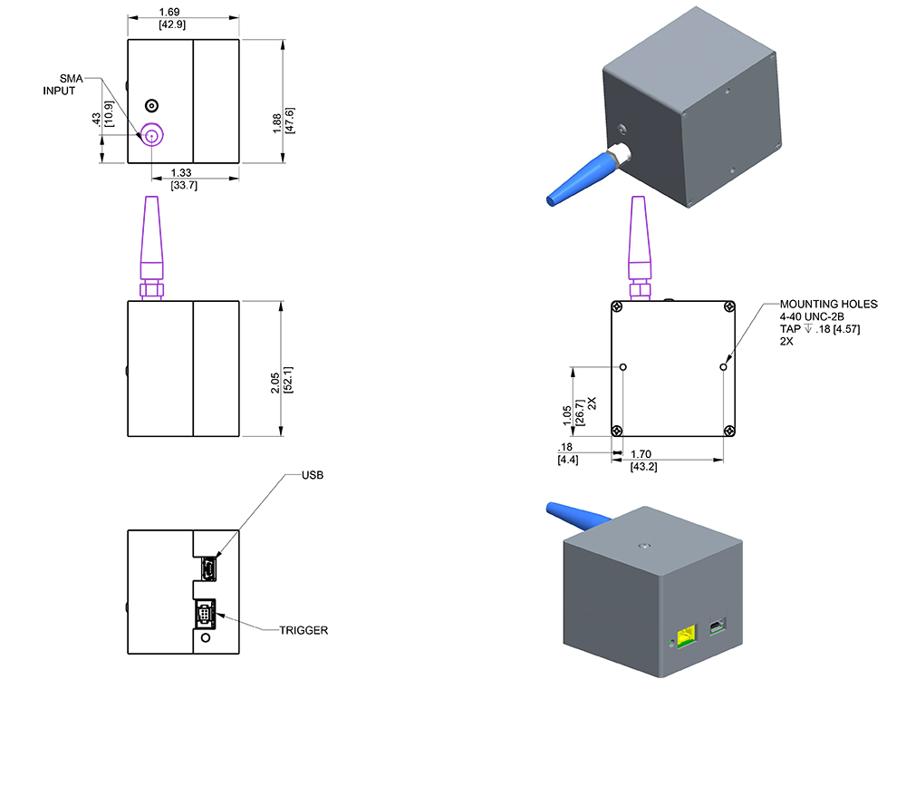
HORIBA designs and manufactures miniature high-throughput OEM spectrometers from 190 nm to 1700 nm for various applications. Thanks to a low stray light aberrations corrected concave holographic grating, the VS20-SYS platform offers in a 1.68 x 1.87 x 2 inches footprint a very reliable and robust spectrometer.
VS20 OEM spectrometers can be fully customized in sensors, entrance, slit size, electronics board, interface, etc.
For OEM Industrial Applications
ㆍ Fluorescence
ㆍ Transmission and Reflectance
ㆍ Examples :
- Semiconductor Process Inspection
- LED Testing
- Color Measurement
- Environmental monitoring
- Food & Beverage Safety
ㆍ Very compact and robust
ㆍ Cost effective OEM solution
ㆍ Mass production capability
ㆍ Various wavelength ranges UV/VIS/VNIR/NIR
ㆍ Low stray light
ㆍ Customizable to customers'requirement
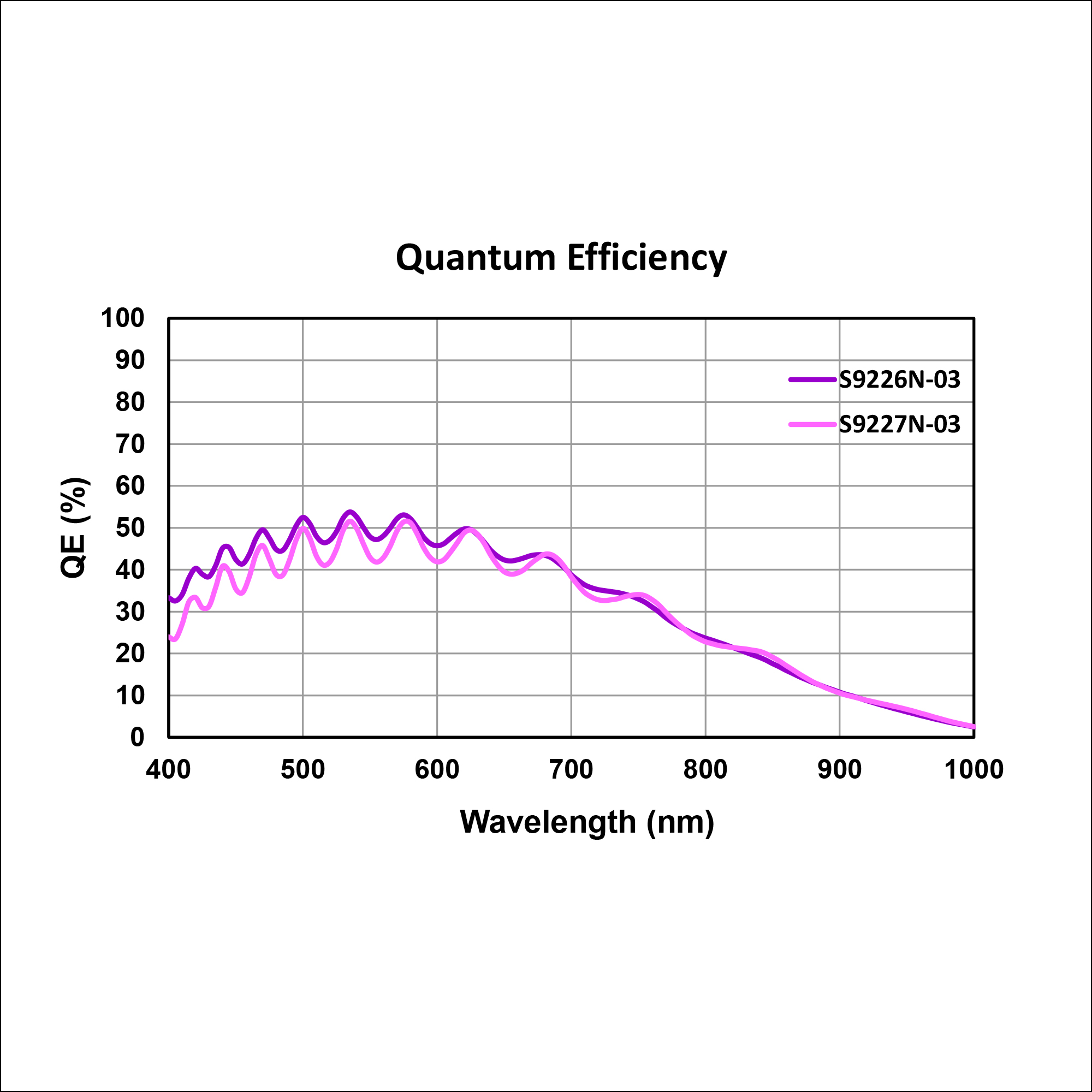
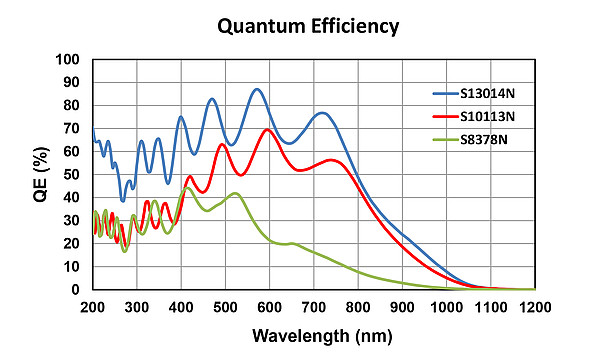
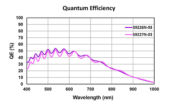
Quantum Efficiencies
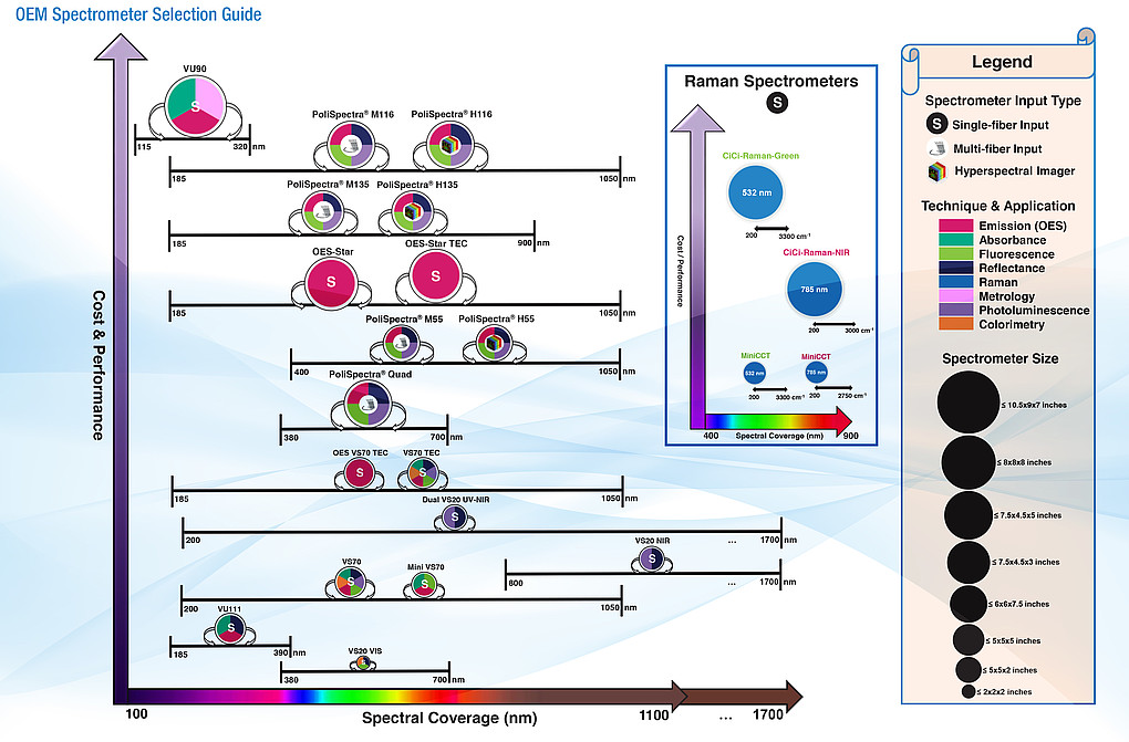
OEM Spectrometer Selection Guide
General Spectrometer Specifications
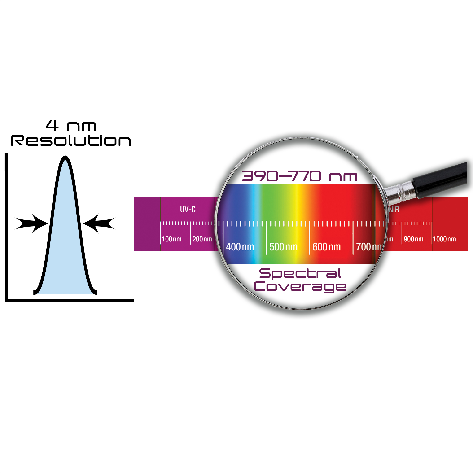
| Spectral Coverage | 390 – 770 nm extending to UV or NIR range is possible upon request |
| Spectrometer Resolution | <4 nm with 50 μm slit width (Narrower slits available) |
| Spectral Dispersion | 56.51 nm/mm (in average); 0.44 nm/pixel |
| Focal Length | 20 mm |
| Options | Selection of different high grade sensors : CMOS-APS*, CMOS-PPS** (PDA), optional CCD on request Input port: SMA, other options available upon request |
| F/# | ~ F/2.7 |
| Wavelength Accuracy | <0.4 nm (using multi-area wavelength calibration) |
| Stray Light | < 0.15% |
| Software | LabVIEW™ acquisition software for initial evaluation (DLLs provided for software integration) |
Detector Options and Specifications
| Detector Type | Hamamatsu CMOS-APS linear image sensor S13014N with active pixel structure and global e-shutter |
Other detector options such as CMOS-PPSs with passive pixel structure and full well up to several 100,000,000 e– and back illuminated CCDs available upon request. See some options in the table below. |
| Detector Sensor Format | 512 x 1 pixels | |
| Detector Pixel Size | 14 μm x 200 μm | |
| Detector QE | refer to graphs below | |
| Full Well Capacity | 100,000 e¯ (typical) 80,000 e¯ (minimum |
|
| Readout Noise | 16 e¯ (typical) to 20 e¯ (maximum) |
|
| Maximum Spectral Rate | 44 spectra/s | |
| ADC | 16-bit | |
| Dynamic Range (FW/RN) | 7053:1 | |
| Non-linearity | <1% (corrected) | |
| Dark Current | 375 e¯/pixel/s (typical) 500 e¯/pixel/s (maximum) |
|
| Communication | USB 2 | |
| Environmental Conditions | Operating temperature 0°C to 40°C ambient Relative humidity <70% (non-condensing) Storage temperature -25° C to 45° C |
|
| Power Requirements AC/DC Power Supply (provided) |
90-264 VAC, 47–63 Hz |
Some CMOS-PDA Options (other sensors available upon request)
| Sensor type | S10113-256N | S8378-256N | S9226N-03 | S9227N-03 |
| Pixel format | 25μm (W) x 500μm (H) x 256 pixels |
25μm (W) x 500μm (H) x 256 pixels |
7.8μm (W) x 125μm (H) x 1024 pixels |
12.5μm (W) x 250μm (H) x 512 pixels |
| Detector QE | refer to graphs below | |||
| Linear Full Well (e-) | ~94M e- (typical) | ~43M e- (typical) | ~1.9M e- (typical) | ~3M e- (typical) |
| Readout Noise (e-) | 5200 e¯ (typical) | 3370 e¯ (typical) | 390 e- (typical) | 290 e- (typical) |
| Spectrometer housing will be slightly different depending on CMOS-PDA options | ||||
*Specifications, form factor, and spectrometer cover subject to change without notice. No LabVIEW™ license is needed to run our acquisition software.
*APS stands for active pixel sensor CMOS (buried PD, high sensitivity similar to CCD)
**PPS stands for passive pixel sensor CMOS (surface PD, large full well capacity - replaces NMOS-PDAs)
Mechanical Drawings