


지금 보고 계신 제품의 제조사에요
(주)에스에프에이반도체


구매정보
(주)에스에프에이반도체
Assembly and Test, Bumping, 주문형, 포장 반도체 생산, 조립, 검사, 임가공, 화상이미지 전송 칩 제작
연락처
041-520-6400
이메일
gyuho.lee@sfasemicon.com
상품정보에 문제가 있나요?
정보수정 / 삭제요청
코머신은 제품 판매의 당사자가 아닙니다.
제품 상세 정보
이 기업의 다른 제품

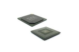
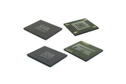
QFP : Quad Flat Package
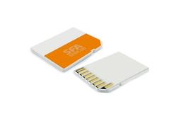
SD Card : Secure Digital Card
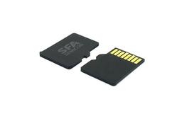
Micro SD Card : Micro Secure Digital Card
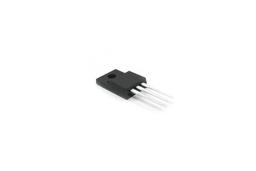
TO-220
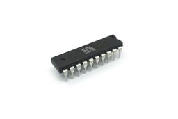
DIP : Dual In-line Package
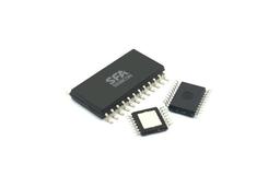
SOP : Small Outline Package
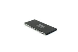
TSOP : Thin Small Outline Package
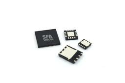
QFN : Quad Flat No Leads
SIP : System in Package
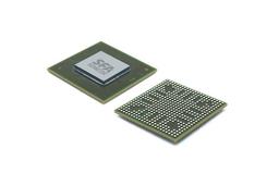
PBGA : Plastic Ball Grid Array
FBGA Stack Die : Fine-pitch Ball Grid Array Stack Die
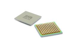
FBGA : Fine-pitch Ball Grid Array
FCCSP : Flip Chip Chip Scale Package
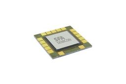
CoC, CoW : Chip on Chip, Chip on Wafer
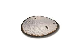
FO-WLP : Fan Out Wafer Level Package


Assembly and Test, Bumping, 주문형, 포장 반도체 생산, 조립, 검사, 임가공, 화상이미지 전송 칩 제작
새롭게 비상하는 SFA 반도체 !!!
SFA반도체는 LSI 및 MEMORY제품을 BUMP에서부터 TEST에 이르는 공정을 일괄생산체제로 구축하여, 생산의 효율성을 강화함은 물론 강도 높은 혁신활동을 통해 끊임없이 기술을 발전시켜 왔습니다.
국내 반도체 Assembly 및 TEST Total Solution NO 1. Provider 로서 만족하지 않고, 세계 최고의 기업으로 도약하기 위해 필리핀과 중국의 해외SITE를 통해 원가 및 품질경쟁력을 확보하였습니다.
이를 바탕으로 Global 고객사들과 Biz.를 안정적으로 확대하였음은 물론, 함께하는 고객사의 경쟁력 강화에도 기여하는 고객만족을 최우선으로 실현해 나가고 있습니다.
SFA반도체는 주주가치 극대화에도 최선을 다하고 있는바, 회사의 가치 향상과 투자자 및 주주여러분들의 이익극대화를 위해 안정된 조직과 투명한 경영시스템을 갖추어 급변하는 경영환경에 효율적으로 대응해 나아가고 있습니다.
SFA 반도체 전임직원은 고객에게는 최고의 기술력을 통한 서비스, 주주에게는 이익극대화를 통한 주주가치제고, 사원들에게는 신나게 일할 수 있는 최고의 직장을 제공할 수 있도록 항상 노력하겠습니다.
대한민국을 대표하는 OSAT 회사로 새롭게 비상하는 SFA 반도체를 아끼고 성원해 주시는 모든분들께 감사의 말씀을 전하며, 앞으로도 따뜻한 관심과 사랑을 부탁 드립니다.